


- Scanning electron microscopy imaging in secondary and backscattered modes with nanometer resolution.
- Scanning Transmission electron microscopy imaging in different modes.
- Preparation of electron-transparent lamellae for TEM/STEM studies from any type of organic/inorganic materials, starting from bulk samples and selecting the regions of interest with nanometer resolution through ion beam milling and thinning.
- Structural (SEM, BSE) and analytical (XEDS) Tomography of micrometer-sized volumes using the slice and view (FIB tomography) technique.
- Phase and orientation mapping using Electron Backscattered Diffraction maps.
- Nanopatterning using Ga+ ion beams.
- Accelerating voltage (electrons): 200 eV to 30 keV (20 eV landing energy with Beam Deceleration)
- Electron beam current: 1 pA to 400 nA
- Resolution (with electrons): 0.7 nm at 30 kV (STEM), 1.0 nm at 30 kV (SEM), 1.4 nm (1.2 with beam deceleration) at 1 kV (SEM)
- Accelerating voltage (Ga+ beam): 500 V to 30 kV
- Ion beam current: 1.5 pA – 65 nA
- Resolution (Ga+ beam): 3.0 nm
- Pt, C and selective carbon mill gas injectors
- 5-axis motorized stage
- EasyLift EX nano-manipulator with orthogonal axis and motorized compucentric rotation navigation system.
- Fully automized FIB lamellae preparation through AutoTEM4 software
- AutoSlice and View image and analytical software packages.
- Oxford instruments Ultim Extreme 100 mm2 detection area XEDS system
- Oxford instruments C-Nano EBSD system
- Integrated Plasma Cleaner
- Cryo-stage for operation at L-N2 temperature.
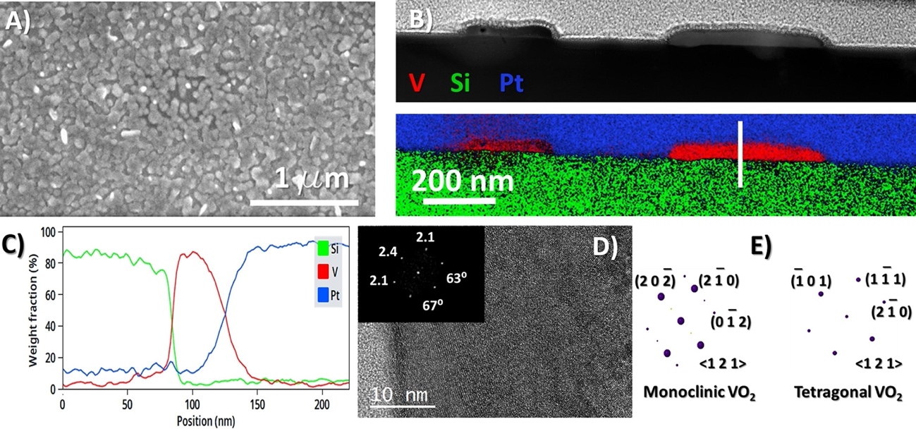
STEM characterization of thin-films. Thermochromic VO2-Boroflat smart glasses. (A) SEM image; (B) HAADF and composite elemental map from a FIB lamellae prepared in cross-section; (C) line profile analysis; (D) HREM image of the VO2–Borofloat glass substrate interphase and digital diffraction pattern (inset); (E) simulated electron diffraction patterns of two different VO2 phases under kinematic conditions.
https://doi.org/10.1016/j.apsusc.2021.152228
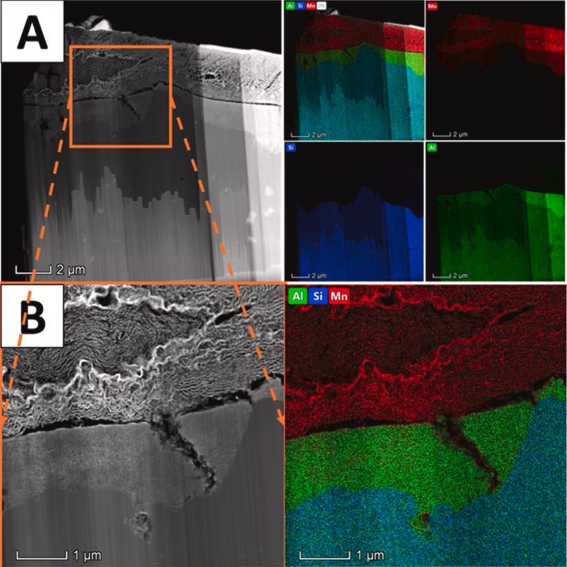
Nanoscopic and atomic scale characterization of catalytic devices. Combining lamellae preparation by FIBSEM and STEM studies for the analysis of washcoating-layers in honeycomb-type catalytic monoliths. (a) STEM-HAADF image of a lamella prepared from a Mn-Cu/Cordierite monolith. XEDS maps of the different elements involved in the system are shown at the right; (b) Detail of the Mn-CuOx catalyst porous washcoated layer and STEM-XEDS analysis showing intermixing of Al2O3 and Mn-CuOx during the washcoating process.
https://doi.org/10.1016/j.apsusc.2021.150318
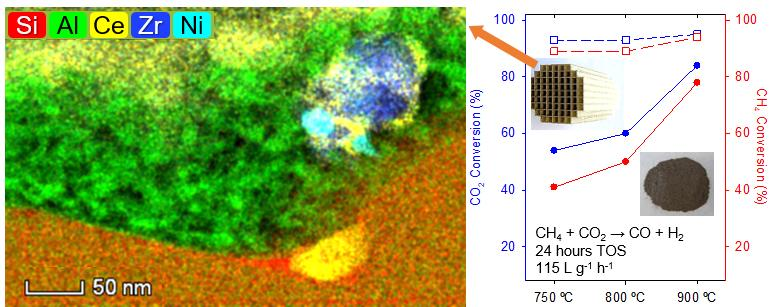
Nanoscopic and atomic scale characterization of catalytic devices. Combining lamellae preparation by FIBSEM and STEM studies for the analysis of CeO2-ZrO2 washcoating-layers in highly stable honeycomb-type monoliths for Methane Dry Reforming. The composite STEM-XEDS map shown at the right allows determining the spatial distribution of the different components of both the monolith substrate and the wascoated catalysts with subnanometric resolution.