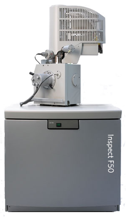
FIELD EMISSION SCANNING ELECTRON MICROSCOPE CSEM-FEG INSPECT 50
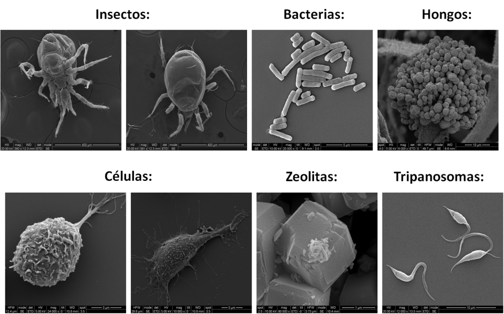
A scanning electron microscope (SEM) is a type of electron microscope that produces images of a sample by scanning it with a focused beam of electrons. The electrons interact with the sample, producing various signals that can be detected in the electron microscope detectors giving information about surface topography and composition of the sample.
The Inspect F-50 SEM instrument is a general-purpose field-emission Scanning Electron Microscope for high-resolution imaging and composition analysis by energy-dispersive X-ray microanalysis (EDS).
What can be done with it?
Image / Analysis
By using the different SEM Detectors with which this instrument is equipped, the following information can be obtained:
- Images with secondary electrons image and topography by means of an ETD (Everhart-Thornley Detector).
- Image and composition by using a BSED (Back Scattering Electron Detector).
- Elemental chemical analysis by means of Energy-dispersive X-ray spectroscopy (EDX).
Sample requirements:
Liquid and non-conductive samples observed need to be dried and metallized prior to observation. Samples studied at low vacuum can be used without metallization at low voltage (low contrast and low sharpness images).
Types of samples that can be studied with Inspect F-50 SEM include:
- Conductive and non-conductive samples, bulk, films, coatings, powders (compacted), etc.
- Samples compatible with high vacuum conditions.
- Sample Diameter from less than 1 mm up to 50 mm.
Technical specifications:
- SEM
- 1 kV: 3.0 nm without BSED
- 30kV: 1.0 nm
- Maximum beam current: 200 nA
- VACUUM
- High vacuum (only mode)
- X x Y x Z (mm): 50 x 50 x 50 mm
- STAGE
- Tilt -15º a 75º
- Rotation: 360º
- DETECTION
- Solid state BSE: BSED
- ETD: SE