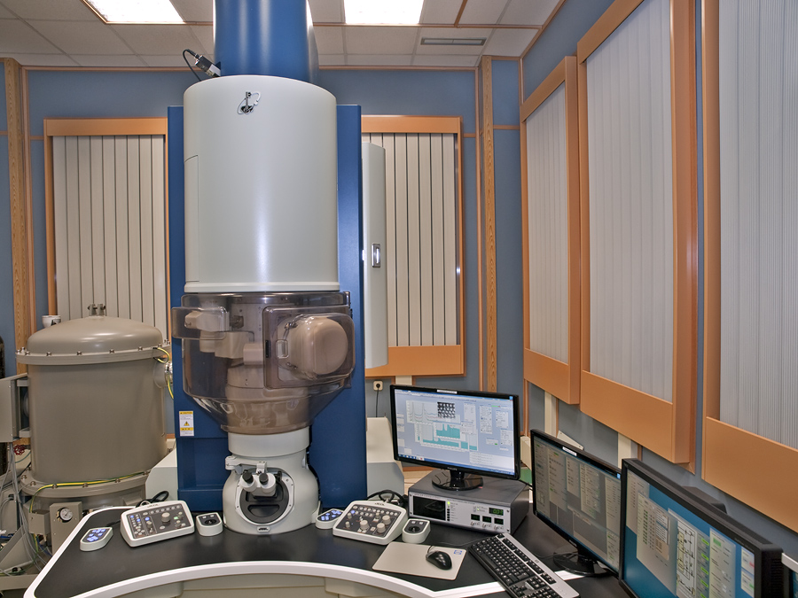
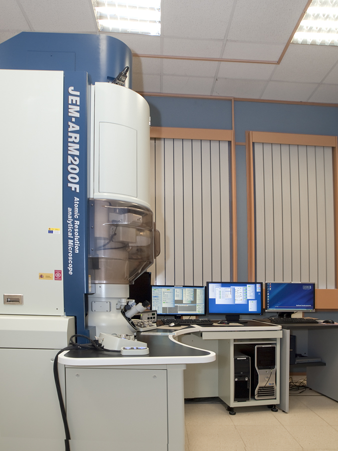
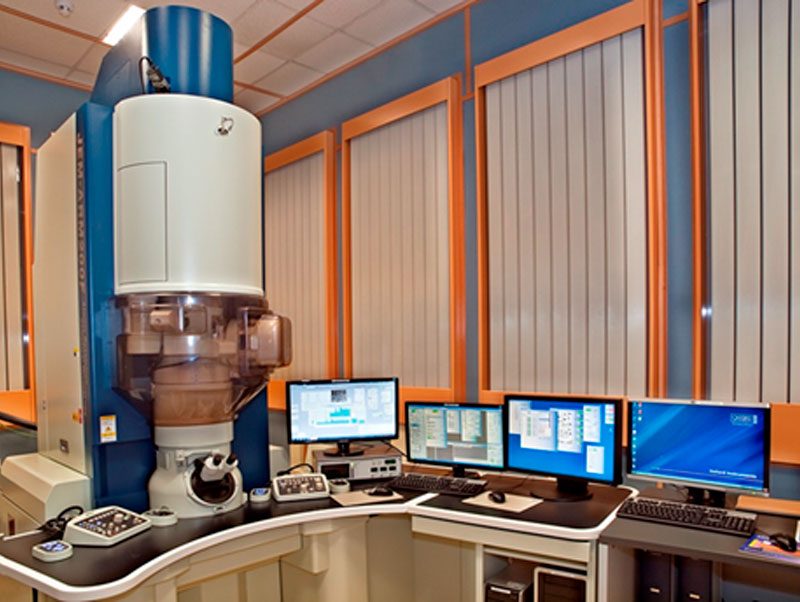
Electron Microscope JEM ARM200cF
The JEOL JEM ARM200cF located at the National Centre for Electron Microscopy (CNME) is unique in Spain. This microscope features make it particularly suitable to study structural, chemical and electronic properties of materials at atomic resolution. Its main characteristics are:
- Cold Field Emission Gun, which delivers a very high intensity beam of sub-angstrom size and energy spread bellow 0.5 eV.
- Spherical aberration corrector CEOS CERCOR, located at the condenser lens, which allows achieving sub-angstrom resolutions when the microscope is used in Scanning-Transmission Electron Microscopy mode, STEM.
- Bright and Dark field detectors, possessing the capacity to gather information about both light and heavy elements with atomic resolution.
- The microscope can be operated at 200, 120 and 80 kV, which allows to carefully adjust experimental conditions to be able to study materials sensitive to the electron beam. Additionally, the usage of low voltages combined with a precise control of electron dose conditions avoids the modification of oxidation states.
- Image Filter Gatan GIF Quantum ER with Dual EELS (Electron Energy Loss Spectroscope), with a series on lenses capable of correcting aberrations up to 5th order. This allows using high collection angles (>100 eV), being able to accomplish energy resolutions of ~3 eV. For these reasons, JEM ARM 200cF is especially recommended for the so called “analytical microscopy” experiments, whose purpose is the study of atomic compositions, oxidation states, atom coordination, projected band structure around the Fermi level, etc.
STEM Images (spatial resolution 0.078 nm):
HAADF images: analytical information about heavy elements with atomic resolution:
Scattered intensity at high angles (between ~ 70 y 200 mrad) is collected, and the image contrast is almost proportional to Z2. Hence, in images acquired using this mode, heavy elements appear brighter than lighter elements on a dark field, being possible to distinguish elements by their intensity. Therefore, HAADF images interpretation is more straightforward than phase contrast-based microscope modes, such as HRTEM, and, additionally, they can provide qualitative analytical information. This technique is particularly useful when combined with EELS because both EELS spectra and HAADF images can be simultaneously acquired, atomic column by atomic column. This allows generating compositional maps which can be employed to unequivocally locate chemical elements with atomic resolution.
ABF images: light elements information, and the study of crystallographic distortions:
Scattered electrons at intermediate angles (between ~ 10 y 20 mrad) are collected. Image contrast is inverse to HAADF images: chemical elements appear in different shades of grey (brighter as lighter the elements) on a bright field. Therefore, both light and heavy elements can be imaged. Hence, this technique is extremely relevant for complex oxides studies as it can reveal M-O bond distortions, atomic displacements, allow the identification of elements as light as H, Li, etc.
Chemical Analysis:
- Compositional studies by spectroscopic techniques: X-EDS (X-ray energy dispersive spectroscopy) and EELS.
- Single analysis, spectrum-image and energy filtered (EFTEM) modes:
- Single analysis both in TEM and STEM modes.
- Spectrum-image: spectra acquisition along lines and areas, collected at each position of the electron probe. With this technique compositional profiles and chemical maps can be gathered. Simultaneous HAADF and EELS acquisition allow the exact correlation between spectroscopic and structural information on the as analyzed area.
- EFTEM images: a parallel electron beam is employed, and transmitted electrons are split via a magnetic prism, selecting those with a specific energy.
- Oxidation state and coordination determination in transition metals via EELS: fine structure of absorption peaks, ELNES (Energy Loss Near Edge Structure). ELNES corresponds to the high intensity region of an EELS spectrum, extending from its threshold up to the first 30-40 eV of each peak within the core loss region. The fine structure describes the possible electronic states above the Fermi level in an atom when it ionizes, providing information about its electronic and local crystallographic structures.
- Low loss region analysis, in order to study the band gap and plasmon energies of different materials, allowing the determination of their optoelectronic properties.
- Cold field emission gun (cFEG).
- Acceleration voltages: 200, 120, 80 kV.
- Objective lens (TEM): focal distance 1.9 mm, Cs 0.5 mm, Cc 1.1 mm, minimum focus step 25 nm.
- Objective lens (STEM) Cs 0.1 at 0.6 mm, Cc 1.4 mm.
- Magnification range (TEM): 2,000x – 2,000,000x.
- Magnification range (STEM) 20,000x – 150,000,000 x.
- Camera length range: 80 – 2,000 mm.
- Specimen tilt range: ±25 degrees.
- STEM spatial resolution: 0.078 nm at 200 kV; 0.136 nm at 80 kV.
- TEM spatial resolution: 0.10 nm lattice, 0.19 nm point to point at t200 kV.
- Gatan Quantum Dual EELS with a high energy resolution of 0.35 eV.
- Gatan OneView camera: from 4096×4096 pixels at 25 fps to 512×512 pixels at 300 fps, for fast image acquisition and in-situ
- STEMx for 4D STEM.
- XEDS Oxford X-MaxN 100 TLE detector.
- Windowless detector.
- SSD detector, Silicon Drift Detector, peltier cold type.
- Detection area: 100 mm².
- Spectra and compositional maps acquisition via AzTecTEM and Digital Micrograph software, allowing the simultaneous acquisition of both EELS and XEDS data.
- Resolution of 129 eV using EDS (measured in Mn-Kα line).
Techniques development/optimization
- A microscopy technique sensitive to the local magnetic field has been developed, energy-loss magnetic chiral dichroism (EMCD). This technique, with high resolution in real space, has been optimized for the optics of JEOL ARM200cF.
- In-situ techniques are applied in order to modify nanomaterials and to study their evolution in real time while being submitted to external stimuli, such as temperature or magnetic fields.
- STEM-X: performing 4D STEM can be achieved by the usage of both the STEM-X system and one view camera. This allows the acquisition, at each electron probe position, of a 2D diffraction pattern, generating a 4D data cube whose ulterior analysis provides numerous information about the materials: diffractometric, orientation and strain maps, defects, etc.
All these techniques allow the visualization of periodic distortions, the identification of local order and dopant alterations, the determination of oxidation states, etc. This can be achieved by a deep analysis of compositional maps and of images of crystallographic distortions and local displacements. Additionally, it can help unveil the functional behavior or advanced materials with diverse dimensionalities (1D, 2D, and 3D), both as thin films or polycrystals (bulk and nano), such as ferroelectrics, magnetics, catalysts, etc.
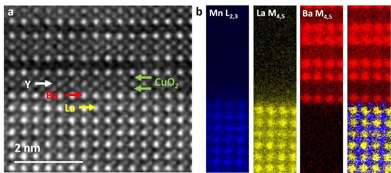
(a) Atomic resolution HAADF image where atomic positions of each element are indicated by arrows in the different atomic columns.
(b) Ba M4,5 (red), Mn L2,3 (blue) and La M4,5 (yellow) elemental EELS map and color mix of a spectrum image of a region of interest from the same HAADF image. Figura adaptada de Nature Materials 21, 188-194 (2022) (doi: 10.1038/s41563-021-01162-5).
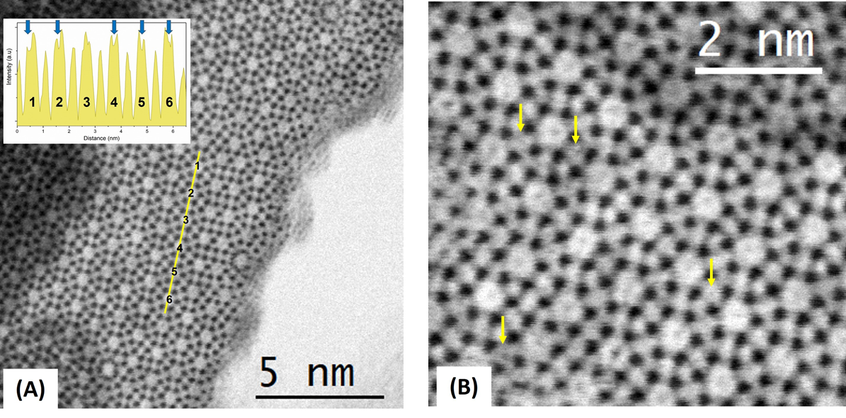
ABF-STEM micrographs showing the arrangement of novel h’-H0.07WO3 bronze. The inset in (A) shows contrast variations along the yellow line. Each large increase in intensity corresponds to each numbered (WO6)6 tunnel along the line. Blue arrows show depressions of intensity in each tunnel, highlighting inserted light cations. The arrows in (B) points dark contrast in some of the (WO6)4 channels. Adapted from Nature Communications 10 (1), 1-9, 2019.
Some recent publications about advanced materials employing this electronic microscope
Jacobo Santamaría et al. “Extremely long-range, high temperature Josehpson coupling across a half-metallic ferromagnet”, Nature Materials, 21, 188, 2022.
J. Villalva et al. “Spin-state-dependent electrical conductivity in single-walled carbon nanotubes encapsulating spin-crossover molecules”, Nature Communications 12(1), 1 2021.
S. Estandía et al. “Insights into the atomic structure of the interface of ferroelectric Hf0.5Zr0.5O2 grown epitaxially on La2/3Sr1/3MnO3”, Phys. Rev. Materials, 5, 074410, 2021.
I. Gómez-Recio et al. “Exceptional Low-Temperature CO Oxidation over Noble-Metal-Free Iron-Doped Hollandites: An In-Depth Analysis of the Influence of the Defect Structure on Catalytic Performance”, ACS Catalysis. 11, 15026, 2021.
W. S. Paz et al. “Franckeite as an Exfoliable Naturally Occurring Topological Insulator,” Nano Lett. 21, 7781, 2021.
H. Li et al. “Strongly Anisotropic Strain‐Tunability of Excitons in Exfoliated ZrSe3,” Adv. Mater. 34(1), 2103571, 2021.
M.W. Yoo et al, “Large intrinsic anomalous Hall effect in SrIrO3 induced by magnetic proximity effect”, Nature Communications. 12, 3283, 2021.
D. del Pozo-Bueno et al. “Direct evidence of a graded magnetic interface in bimagnetic core/shell nanoparticles using electron magnetic circular dichroism (EMCD)”. Nano Letters 21, 6923, 2021.
D. Hernandez-Martin et al. “Controlled Sign Reversal of Electroresistance in Oxide Tunnel Junctions by Electrochemical-Ferroelectric Coupling,” Phys. Rev. Lett. 125, (26), 266802, 2020.
J. Oró-Solé et al. “Engineering Polar Oxynitrides: Hexagonal Perovskite BaWON2”, Angew. Chem. 132, 18553, 2020.
C. Franco et al. “Biomimetic synthesis of Sub-20 nm covalent organic Frameworks in water”, Journal of the American Chemical Society. 142, 3540, 2020.
R. Frisenda et al. “Symmetry Breakdown in Franckeite: Spontaneous Strain, Rippling, and Interlayer Moiré,” Nano Lett., 20(2), 1141, 2020.
A. Varela, et al. “Hydroxyapatites as Versatile Inorganic Hosts of Unusual Pentavalent Manganese Cations”, Chemistry of Materials. 32, 10584, 2020.
J. García-Fernández, et al. “Influence of cation substitution on the complex structure and luminescent properties of the ZnkIn2Ok+3 system”, Chemistry of Materials. 32, 6176, 2020.
J. Romero et al. “Giant enhancement in the supercapacitance of Ni-Fe graphene nanocomposites induced by a magnetic field”, Advanced Materials, 31, 1900189, 2019.
Basic information about electron microscopy/aberration corrected microscopy
David B. Williams, C. Barry Carter en Transmission Electron Microscopy. A Textbook for Materials Science. Plenum Press. New York-London (2009).
M. Haider, S. Uhlemann, E. Schwan, H. Rose, Nature 392, 5 (1998).
O. L. Krivanek, P. D. Nellist, N. Dellby, M.F. Murfitt, Z. Szilagyi. Ultramicroscopy 78, 1 (1999).
Rolf Erni en Aberration-Corrected Imaging in Transmission Electron Microscopy An Introduction. Imperial College Press. London (2010).
Aberration–Corrected Analytical Transmission Electron Microscopy. Editado por R. Brydson. John Wiley&Sons (2011).
Information about ABF images
S. D. Findlay, N. Shibata, H. Sawada, E. Okunishi, Y. Kondo, T. Yamamoto, Y. Ikuhara, Appl. Phys. Lett. 95, 200895 (2009).
S. D. Findlay, N. Shibata, H. Sawada, E. Okunishi, Y. Kondo, Y. Ikuhara Ultramicroscopy 110, 903 (2010).
Basic information about EELS
[35] R. F. Egerton, en Electron Energy-Loss Spectroscopy in the Electron Microscope, Plenum Press. New York-London (1996).
Rik Brydson, en Electron Energy Loss Spectroscopy, Taylor & Francis (2001).
Oxidation states determination via EELS
M. Varela, M. P. Oxley, W. Luo, J. Ç. Tao, M. Watanabe, A. R. Lupini, S.T. Pantelides, S. J. Pennycook Phys. Rev. B 79, 085117 (2009).
H. Kurata and Christian Colliex. Physical Review B 48 (4), 2102-2108 (1993).