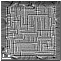
Magnetic materials
Magnetic materials have attracted the attention and stimulated the imagination of Humankind since the discovery of the attractive properties of lodestone in Ancient China. The potential for practical applications of this “magic” force was soon put in action. The invention of compass in the Middle Ages was just the first of multiple uses of magnetic materials that have contributed to change the world we live in, including the development of electricity in the XIX century or the ultra-high density information storage media in late XX. The most recent advances in magnetic materials are related to the emergence of two disciplines intimately related: Nanomagnetism and Spintronics.
New phenomena arise when the physical scale of a magnetic material is reduced down to the nanometric scale, at the threshold between the classical macroscopic world and the quantum phenomena dominating in the range of atomic distances. The magnetic properties of nanoparticles, nanowires or thin films can be drastically different from that of their macroscopic counterparts by the combined effect of the scale reduction and the increasing relevance of surfaces and interfaces. The most remarkable exploitation of the magnetic phenomena at the nanoscale is the development of Spintronics, which relies on the possibility of controlling two main physical properties of the electron, charge and spin, assisted by the use of spin-polarized currents. Spintronics has flourished as one of the main areas of Magnetism for both fundamental research and applications in the fields of information storage and processing, and is intimately related to Nanomagnetism, as most of these phenomena are manifested at the nanoscale in thin films or nanopatterned magnets.
TEM Magnetic Imaging: Lorentz Microscopy and Electron Holography
One of the main issues to understand the deep physical origins of magnetic phenomena at the nanoscale is the accurate determination of the magnetic configurations of nanomagnets, and the analysis of their dynamics as a function of external parameters such as electromagnetic fields or temperature. In this field, Transmission Electron Microscopy provides two different techniques magnetic imaging of magnetic structures with spatial resolution in the range of nanometers: Lorentz microscopy and off-axis Electron Holography, which are intimately related.
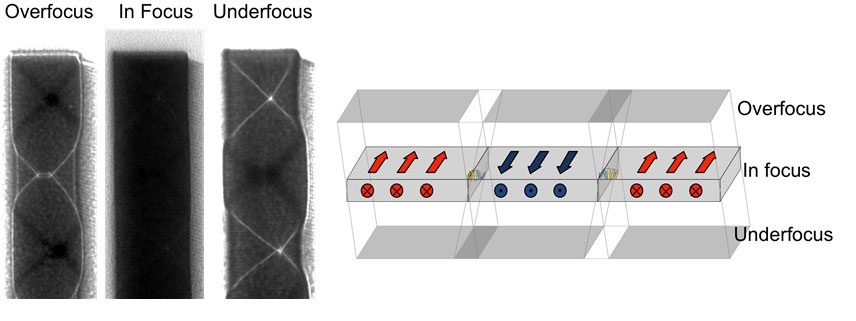
Figure 1. Lorentz microscopy in Fresnel mode
The most straightforward magnetic TEM imaging technique is Lorentz microscopy. Although it presents multiple variants, Lorentz microscopy in Fresnel mode is by far the most widely used. Defocused Fresnel images present magnetic contrast (bright/dark lines) at the position of the magnetic domain walls, the strength of this contrast depending on the relative orientation of the magnetization at both sides of the domain wall. The application of the Transport-of-Intensity Equation (TIE) formalism to focal series of Fresnel images enables the retrieval of the magnetic phase shift of the electron wave, which is directly related to the in-plane magnetic induction. Thus, TIE allows the quantitative mapping of the magnetic induction produced by the nanomagnet.
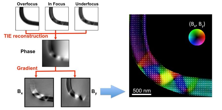
Figure 2. Transport-of-Intensity (TIE) procedure
Off-axis Electron Holography is a more sensitive and quantitative TEM technique sensitive to magnetism. Relying on the interference between a wave interacting with the sample and an unperturbed wave via a negatively biased metallic wire called electron biprism, different strategies can be followed to extract the phase shift of the electron wave induced by the magnetic induction around the sample. The magnetic information can be fully quantitative and enables the mapping of the magnetic induction created by a nano-magnet. An example of holographic reconstruction of the electrostatic and magnetic phases is shown in Figure 3 (Electron Holography).
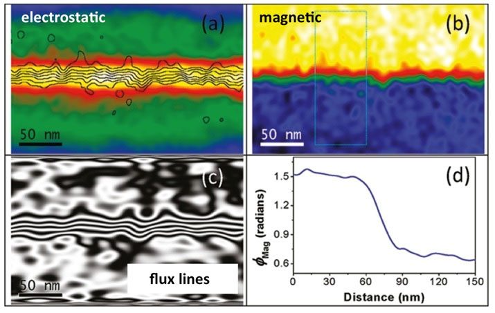
Figure 3. Electron holography reconstruction of (a) the electrostatic phase shift, and (b) the magnetic phase shift of the electron wave of an ultrathin Co nanowire. (c) Magnetic flux lines confined inside the nanowire. (d) Profile of the magnetic phase shift perpendicular to the nanowire.
In situ magnetic imaging in TEM
Both techniques require that the sample be in field-free conditions in order to probe the magnetism of the specimen. As the objective lens of a modern microscope applies a magnetic field of approximately 2 T in the sample position, this field would saturate the magnetization of most ferromagnets. Thus, it is required to switch off the objective lens and use an auxiliary focusing lens, the Lorentz lens. It is located immediately below the objective lens and produces a small field in the sample. However, the possibility of applying magnetic fields inside the electron microscope is paramount to probe the magnetic properties of nanomaterials, as it enables the realization of magnetic hysteresis loops in nano-objects to investigate magnetization reversal processes in nanostructures. In this field, we have developed a generalized procedure to apply magnetic field in the sample by slightly exciting the objective lens while tilting the sample. This way, in magnetic specimens with high in-plane shape anisotropy where strong demagnetizing fields makes the out-of-plane component of the external field negligible, we can manipulate the magnetization states of the sample applying controlled in-plane magnetic fields along an arbitrary direction and with amplitudes up to 2000 Oe. This requires a careful calibration of the magnetic field applied by the objective lens as a function of the electric excitation, which has been carried out with a TEM holder equipped with a Hall probe in the sample position. The result of this calibration can be seen in Figure 4.
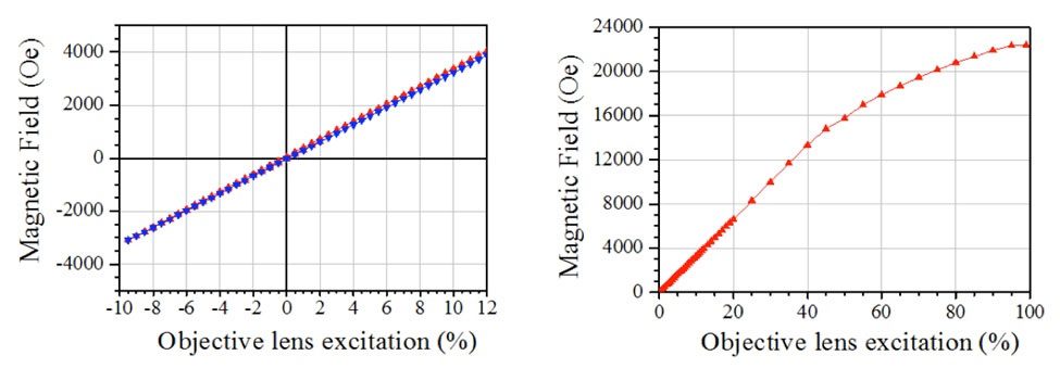
Figure 4. Calibration of the magnetic field applied by the SuperTwin objective lens of the FEI Titan Cube.
Figure 5 (Video). Manipulation of superdomain walls along a cobalt antidote array with the magnetic field applied with the objective lens.
The control on the magnetic field we apply to our sample inside the TEM has enabled multiple studies related to the study of magnetic reversal processes of nanostructures For instance, we have carried out a complete characterization of the magnetic nucleation and propagation of domain walls in an array of cobalt antidots, which is a cobalt film where a periodic pattern of holes has been created. The nucleation and propagation of superdomain walls inside the antidot structure was carried out using our newly developed procedure for applying magnetic fields and observing the change in contrast of the Fresnel fringes (click on the video in Figure 5).
There are other possibilities of in situ TEM in the field of magnetism, such as temperature-dependent TEM. Using a dedicated cooling sample holder in the FEI Titan Cube, temperature dependent magnetic states can be characterized in situ by Lorentz microscopy and Electron Holography. An example of this application is the observation of magnetically dead layers in strained La0.66Ca0.37MnO3 (LCMO) thin films. Depending on the growth conditions and the relative deformation of the lattice induced by epitaxial strain, LCMO films can be fully magnetized at 100 K (below the Curie temperature), or be partially non-magnetic at the free surface of the film.
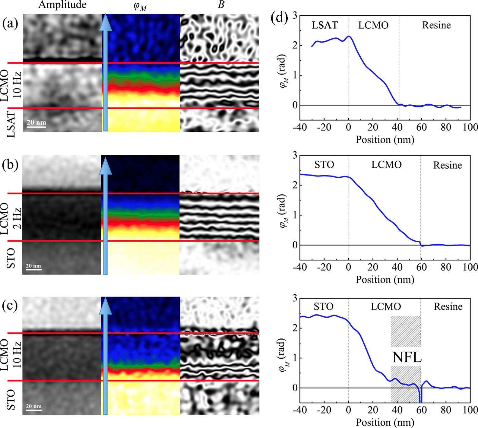
Figure 6. Observation of magnetically dead layers in strained LCMO thin films by in situ electron holography at 100 K.
Characterizing new magnetic nanostructures by magnetic TEM Imaging
The development of new functional ferromagnetic nanostructures requires an intensive local characterization of its magnetic properties, and magnetic TEM imaging plays a key role in the quantitative visualization of the magnetization states at the nanoscale.
A paramount example of this is the design of novel magnetic nanostructures by synthetic techniques such as Focused-electron-beam-induced deposition (FEBID). FEBID is considered the ultimate direct-write lithography technique for three-dimensional (3D) structures. However, it has not yet been possible to obtain 3D deposits by FEBID with the same purity and crystallinity of the corresponding bulk materials. To obtain bulk-like 3D deposits, the purification of the nanostructures by high temperature thermal annealing up to 600ºC is required after FEBID growth. Advanced TEM techniques, in particular Electron Holography, have evidenced that the annealing process improves the magnetization of the nanowires up to virtually bulk, by inducing a purification and crystallization process that transforms the pseudo-amorphous 3D nanowires into pure (>95 % at. Co) crystalline nanowires. This achievement opens new pathways for applications of this synthetic method in the fabrication of either individual or arrays of 3D high-purity and crystalline Co nanowires for high-density memory and logic devices, nanosensors, and actuators, and could be a viable method to obtain other pure and crystalline 3D materials by FEBID.
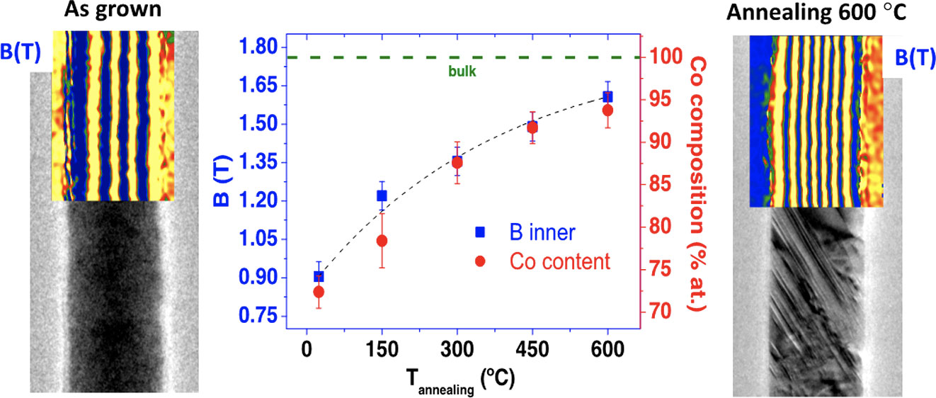
Figure 7. Magnetic induction of as-grown (left) and thermally annealed (right) 3D Co-FEBID nanowires analyzed by Electron Holography.
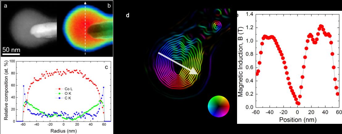
A more direct example of functional applications of FEBID nanostructures is the functionalization of magnetic scanning probe probes. FEBID cobalt nanospheres have been used to optimize the performance of magnetic resonance force microscopy (MRFM) tips, and have been characterized by Electron Holography. Spherical geometries have been achieved with diameters as low as 90 nm, even though such small objects present degraded properties (low Co content). Nanospheres with diameters around 110 nm present optimum cobalt content (similar as their 2D deposits counterparts, approximately 80% at. Co), which guarantees a good ferromagnetic behavior. Due to their spherical nature, Electron Holography measurements have evidenced the formation of a stable magnetic vortex state in remanence, which is ideal for MRFM experiments.
Magnetic characterization of new ferromagnetic nanostructuresIn this work, a detailed investigation of the magnetic properties of cobalt nanospheres grown on cantilever tips by Focused Electron Beam Induced Deposition (FEBID), aimed at functionalizing magnetic resonance force microscopy (MRFM) probes has been carried out by Off-Axis Electron Holography, in combination with analytical Electron Energy Loss Spectroscopy. Spherical geometries have been achieved with diameters as low as 90 nm, even though such small objects present degraded properties (low Co content). Nanospheres with diameters around 110 nm present optimum cobalt content (similar as their 2D deposits counterparts, approximately 80% at. Co), which guarantees a good ferromagnetic behavior. Due to their spherical nature, Electron Holography measurements have evidenced the formation of a stable magnetic vortex state in remanence, which is ideal for MRFM experiments.
Highlights
- Purified and Crystalline Three-Dimensional Electron-Beam- Induced Deposits: The Successful Case of Cobalt for High Performance Magnetic Nanowires. Javier Pablo-Navarro, César Magén and José María De Teresa. ACS Applied Nano Materials 1, 38-46 (2018).
- Magnetic properties of optimized cobalt nanospheres grown by focused electron beam induced deposition (FEBID) on cantilever tips S. Sangiao, C. Magén, D. Mofakhami, G. De Loubens, J. M. De Teresa, Beilstein Journal of Nanotechnology 8, 2106-2115 (2017).
- Observation of the Strain Induced Magnetic Phase Segregation in Manganite Thin Films. L. Marín, L.A. Rodriguez, C. Magén, E. Snoeck, R. Arras, Irene Lucas, Luis Morellón, P. A. Algarabel, J. M. de Teresa, M. R. Ibarra. Nano Letters 15, 492–497 (2015).
- High-resolution imaging of remanent state and magnetization reversal of superdomain structures in high-density cobalt antidot arrays. L. A. Rodríguez, C. Magén, E. Snoeck, C. Gatel, C. Castán-Guerrero, J. Sesé, L. M. García, J. Herrero-Albillos, J. Bartolomé, F. Bartolomé and M. R. Ibarra. Nanotechnology 25, 385703 (2014).
- Quantitative in situ magnetization reversal studies in Lorentz microscopy and electron holography. L. A. Rodríguez, C. Magén, E. Snoeck, C. Gatel, L. Marín, L. Serrano-Ramón, J. L. Prieto, M. Muñoz, P. A. Algarabel, L. Morellon, J. M. De Teresa, and M. R. Ibarra. Ultramicroscopy 134, 144-154, (2013).
- Optimized cobalt nanowires for domain wall manipulation imaged by in situ Lorentz Microscopy. L. A. Rodríguez, C. Magén, E. Snoeck, L. Serrano-Ramón, C. Gatel, R. Córdoba, E. Martínez-Vecino, L. Torres, J. M. De Teresa and M. R. Ibarra. Applied Physics Letters 102, 022418 (2013).
- Ultra-small functional ferromagnetic nanostructures grown by focused-electron-beam-induced deposition. L. Serrano, R. Córdoba, L.A. Rodríguez, C. Magén, E. Snoeck, C. Gatel, I. Serrano, M. R. Ibarra and J. M. De Teresa ACS Nano 5, 7781-7787 (2011).
Laboratorio de Microscopías Avanzadas
Somos una iniciativa singular a nivel nacional e internacional. Ponemos a disposición de la comunidad científica e industrial las infraestructuras más avanzadas en microscopía electrónica y de sonda local para la observación, caracterización, nanoestructuración y manipulación de materiales a escala atómica y molecular.
Datos de Contacto
Campus Río Ebro, Edificio Edificio I+D+i
Enlaces Destacados
© 2021 LMA| Página web desarrollada por o10media | Política de privacidad | Aviso legal | Condiciones de uso | Política de Cookies |


