Nanoparticles and nanomaterials
One of the main research lines in nanoscience relies on the development and study of nanoparticles. In nanotechnology, a nanoparticle is defined as a small object that behaves as a whole unit with respect to its transport and properties with a diameter between 1 and 100 nanometers in size.
One of the main research lines in nanoscience relies on the development and study of nanoparticles. In nanotechnology, a nanoparticle is defined as a small object that behaves as a whole unit with respect to its transport and properties with a diameter between 1 and 100 nanometers in size. Nanoparticles are of great scientific interest as they are, in effect, a bridge between bulk materials and atomic or molecular structures. The properties of materials change as their size approaches the nanoscale and as the percentage of atoms at the surface of a material becomes significant. Often, these materials have unexpected optical properties as they are small enough to confine their electrons and produce quantum effects. Other size-dependent property changes include quantum confinement in semiconductor particles, surface plasmon resonance in some metal particles and superparamagnetism in magnetic materials. For biological applications, Nanoparticles can be linked to biological molecules that can act as delivery tags, so as to direct the nanoparticles to specific sites within the body, specific organelles within the cell, or to follow specifically the movement of individual protein or RNA molecules in living cells. The surface coating of this kind of particles is very important, in order to give high aqueous solubility, prevent nanoparticle aggregation and make the particle functional. The characterization of nanomaterials: morphology, size distribution, coating, physical properties: optical, electrical and magnetic etc. is essential in order to define the nanotechnology applications of this new materials. For this, the most powerful technique is Transmission Electron Microscopy. Different techniques in TEM can provide all the information for a complete characterization of the nanoparticles:
- Morphology, size distribution and coating: C-TEM
- Crystalline information:HRTEM
- Chemical information: Z-Contrast-HAADF imaging, EDS, EELS
- Chemical environment:EELS fine structure
- Optical properties:Studies of surface Plasmon
- Magnetic properties: Lorentz microscopy and Holography
- Electric properties: Holography
- Nanoparticles 3D reconstruction:Tomography
Nanoparticles is one of the most important research lines in INMA-LMA. Some examples of the research involving nanoparticles in our lab are:
Active magnetoplasmonic split-ring/ring nanoantennas – H.Y. Feng, F. Luo, R. Arenal, F. Garcia, G. Armelles, A. Cebollada, Nanoscale 9, 37-44 (2017)
Plasmonic studies on metallic nanostructures: These investigations have been performed by spatially-resolved (SR) high-resolution EELS. In the example reported here, the electromagnetic field distribution at plasmon resonances has been analyzed. The SR-EELS analyses have been performed on Active magnetoplasmonic split-ring/ring nanoantennas that have been produced by the hole-mask colloidal lithography method. In this case, a split Au ring is generated on the bottom Au ring with a Co-dot embedded inside (Fig.).

Figure. HAADF-STEM image of a gapped nanostructure with a 60° gap angle, where the EELS SPIM (c) has been recorded in the area marked with red square. The gap region is clearly seen on the right side of the structure. (b) EEL spectrum collected from the blue marked area (i) in (a), together with the extinction spectrum of the same sample for unpolarized light. (c) The EEL intensity map showing the spatial distribution for the LE mode (red arrow) for this nanostructure. Remarkable enhancement is observed in the gap region, corresponding to the EM field enhancement in this region at the LE plasmon resonance.
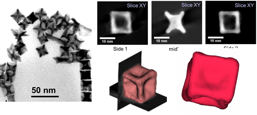
Room temperature synthesis of platinum concave cubes exposing {110} facets and their epitaxial growth on Pt(111) thin films»
Laurent Peres, Deliang Yi, Susana Bustos-Rodriguez, Cécile Marcelot-Garcia, Alexandre Pierrot, Pier-Francesco Fazzini, Bénédicte Warot-Fonrose, Ileana Florea, Raul Arenal, Lise-Marie Lacroix, Thomas Blon, Katerina Soulantica, Nanoscale 10, 22730-22736 (2019) {110}
Bidimensional lamellar assembly by coordination of peptidic homopolymers to platinum nanoparticles.
Ghada Manai, Hend Houimel, Mathilde Rigoulet, Angélique Gillet, Pier-Francesco Fazzini, Alfonso Ibarra, Stéphanie Balor, Pierre Roblin, Jérôme Esvan, Yannick Coppel , Bruno Chaudret, Colin Bonduelle & Simon Tricard.
NATURE COMMUNICATIONS | (2020) 11:2051 | https://doi.org/10.1038/s41467-020-15810-y
A key challenge for designing hybrid materials is the development of chemical tools to control the organization of inorganic nanoobjects at low scales, from mesoscopic (~μm) to nanometric (~nm). So far, the most efficient strategy to align assemblies of nanoparticles consists in a bottom-up approach by decorating block copolymer lamellae with nanoobjects. This well accomplished procedure is nonetheless limited by the thermodynamic constraints that govern copolymer assembly, the entropy of mixing as described by the Flory–Huggins solution theory supplemented by the critical influence of the volume fraction of the block components. Here we show that a completely different approach can lead to tunable 2D lamellar organization of nanoparticles with homopolymers only, on condition that few elementary rules are respected: 1) the polymer spontaneously allows a structural preorganization, 2) the polymer owns functional groups that interact with the nanoparticle surface, 3) the nanoparticles show a surface accessible for coordination. TEM imaging and 3D reconstruction by STEM Tomography have been carried out for the characterization of the samples. Fig. 1.
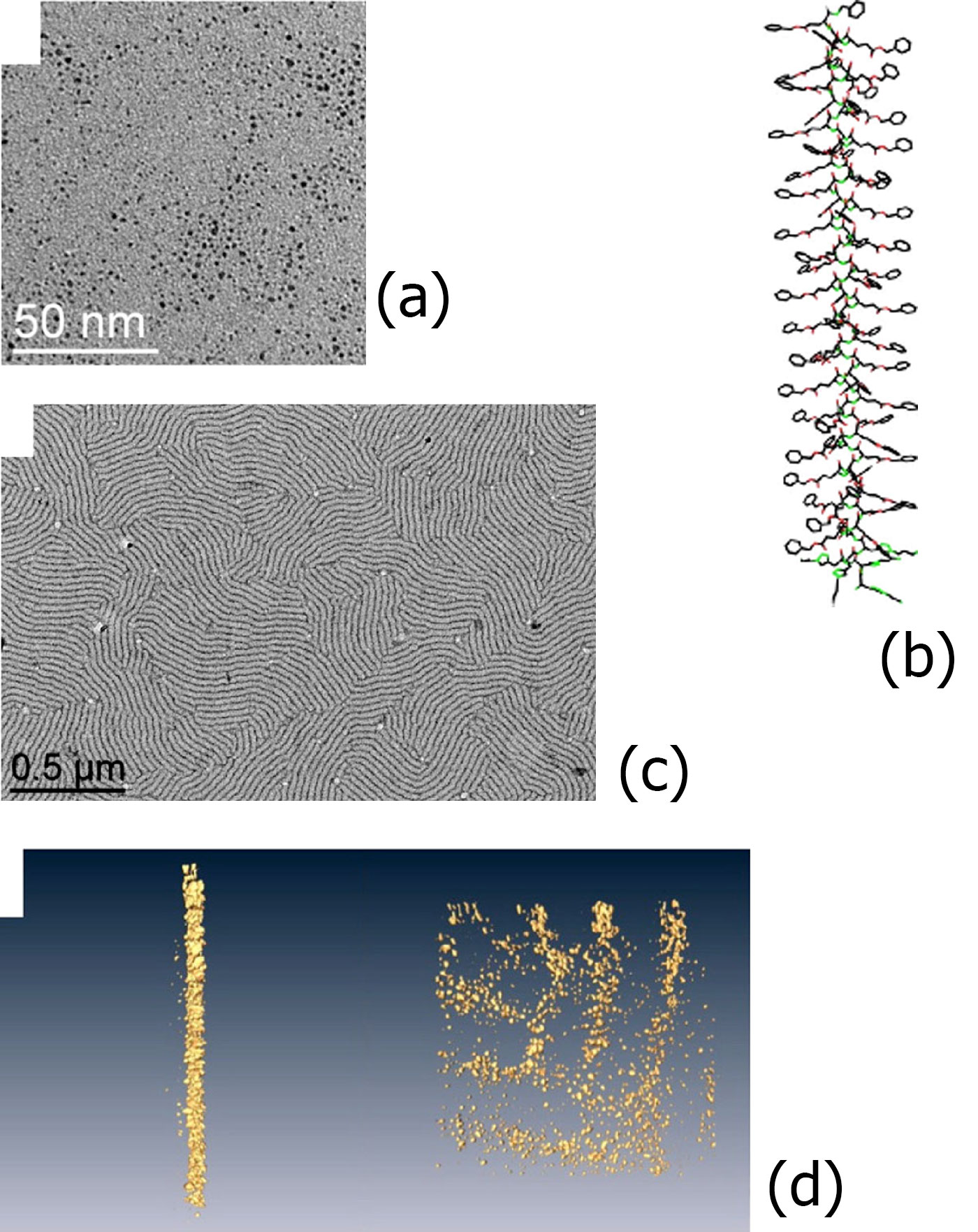
Fig. 1. Building blocks and self-assembly. a TEM image of pristine ultrasmall platinum nanoparticles of 1.2 ± 0.3 nm. b, Geometrical model of the α-helix conformation of PBLG (example for x = 60). Lamellar structuration of an assembly of platinum nanoparticles with PBLG4 at 0.5 eq.: c, Low-magnification TEM image; d, Tomographv 3D reconstruction at two viewing directions: each yellow dot corresponds to an individual nanoparticle.
Unraveling the mechanism of the one-pot synthesis of exchange coupled Co-based nano-heterostructures with high energy product.
Beatrice Muzzi, Martin Albino, Claudia Innocenti, Michele Petrecca, Brunetto Cortigiani, César de Julián Fernández, Giovanni Bertoni, Rodrigo Fernandez-Pacheco, Alfonso Ibarra, Clara Marquina, Ricardo M. Ibarra, Claudio Sangregorio.
Nanoscale, 2020, 12, 14076. DOI: 10.1039/d0nr01361g
The development of reproducible protocols to synthesize hard/soft nano-heterostructures (NHSs) with tailored magnetic properties, is a crucial step to define their potential application in a variety of technological areas. Thermal decomposition has proved to be an effective tool to prepare such systems, but it has been scarcely used so far for the synthesis of Co-based metal/ferrite NHSs, despite of their intriguing physical properties. We found out a new approach to prepare this kind of nanomaterial based on a simple one-pot thermal decomposition reaction of metal-oleates precursors in the high boiling solvent docosane. The obtained NHSs are characterized by the coexistence of Co metal and Co doped magnetite and are highly stable in air atmosphere, thanks to the passivation of the metal with a very thin oxide layer. The investigation on the influence of the metal precursor composition (a mixed iron-cobalt oleate), of the ligands (oleic acid and sodium oleate) and of the reaction time on the chemical and structural characteristics of the final product, allowed us to rationalize the reaction pathway and to determine the role of each parameter. STEM-EELS characterization, Fig. 1 and HRTEM imaging, Fig. 2 and have been performed to know the crystallographic structure of the samples and the core-shell structure respectively.
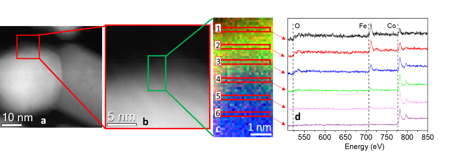
Fig. 1 a) STEM image of a metal NP of NHS-1 and b) magnification of the shell region (5 nm thickness) from the red square in a). c) EELS color mapping of the selected region (ca. 3 x 6 nm) in b panel; this area was chosen as representative of the shell at the metal surface, where the blue and green spots refer to cobalt and iron, respectively. d) Normalized EELS spectra related to the regions in the EELS color map. The peaks at 708 eV and 779 eV correspond to the L2,3 edge of iron and of cobalt, respectively. In the outer surface (region 1 in c), it is possible to distinguish both iron and cobalt edges (intensity 60(6) % and 40(4) %, respectively). Moving towards the inner side (regions 2-6), the iron signal decreases till it disappears (region 6).
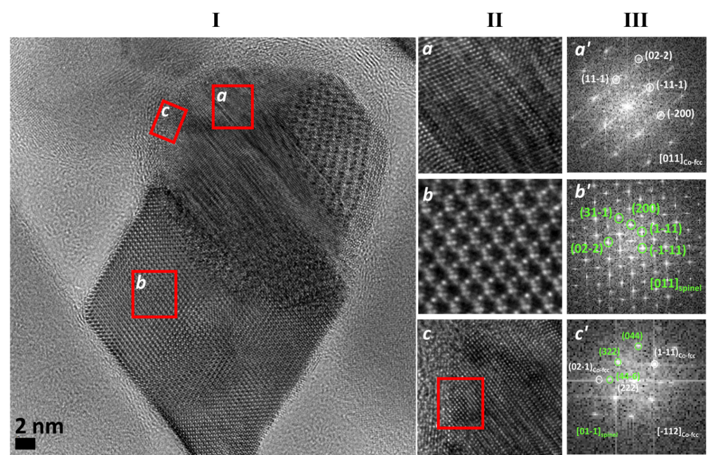
Fig. 2 (I) HRTEM image of a NHS-1 NP, where 3 regions (a, b and c) are selected: a and b correspond to metal and ferrite cores, respectively, while the region c to the shell around the metal core; (II) Enlargement of the selected regions; (III) FFT analysis of the three regions showing the presence of different crystallographic structures: the labelled spots are related to crystallographic planes that can be indexed as: a’) fcc metal phase (), in zone axis [011] [011]Co-fcc, b’) cubic spinel structure (), [011] [011]spinel and c’) metal (white) and cubic spinel oxide (red) [01-1]phases, [01-1]spinel and [-112]Co-fcc; the presence of both phases confirms a sharp interface.
3D superconducting hollow nanowires with tailored diameters grown by focused He+ beam direct-writing
Rosa Córdoba, Alfonso Ibarra, Dominique Mailly, Isabel Guillamón, Hermann Suderow and José María De Teresa. Beilstein J. Nanotechnol. 2020, 11, 1198–1206. doi:10.3762/bjnano.11.104
Currently, the patterning of innovative three-dimensional (3D) nano-objects is required for the development of future advanced electronic components. Helium ion microscopy in combination with a precursor gas can be used for direct-writing of three-dimensional nanostructures with a precise control of their geometry, and a significantly higher aspect ratio than other additive manufacturing technologies.
We report here the deposition of 3D hollow nanowires with tailored diameters by tuning two key growth parameters, namely the ion beam current and dose. Our results show the control of geometry in 3D hollow nanowires, with outer and inner diameters ranging from 36 to 142 nm and from 5 to 28 nm, respectively; and lengths from 0.5 to 8.9 μm. Transmission electron microcopy experiments indicate that the nanowires display a microstructure of large grains with crystalline structure compatible with face-centered cubic WC1-x phase, Fog. 1. In addition, 3D electron tomographic reconstructions depict that the nanowire’s holow center is present along the whole nanowire length, Fig. 2. Moreover, these nanowires become superconducting at 6.8 K and show large critical magnetic field and critical current density. Consequently, these 3D nano-objects could be implemented as components in the next generation of electronics, such as nano-antennas and sensors, based on 3D superconducting architectures.
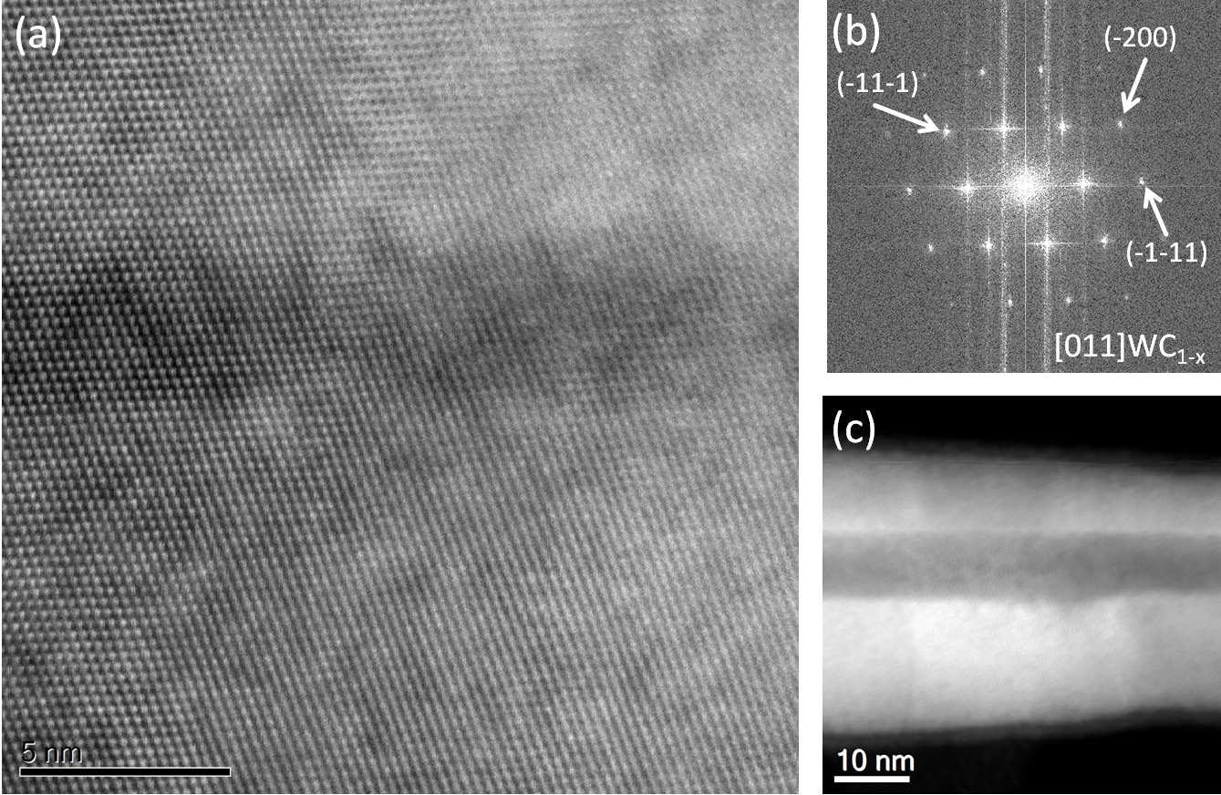
Figure 1: (a) HRSTEM image of a typical WC hollow NW grown at 1.3 pA. (b) Fast Fourier transform of the image in (a), showing the crystalline nature of the material and indexed as the [011] zone axis of the fcc WC1−x structure. (c) Lower magnification STEM image of the WC NW in (a).
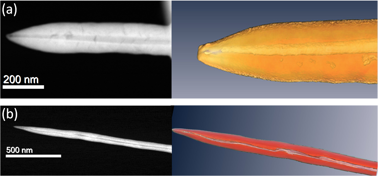
Figure 2: (a) Tomography of WC hollow NW grown at 7 pA, with an outer diameter of 142 nm and inner diameter of 28 nm. Left panel: STEM image. Right panel: Snapshot of the 3D tomographic reconstruction. (b) Tomography of WC hollow NW grown at 2 pA, with an outer diameter of 77 nm and inner diameter of 8 nm. Left panel: STEM image. Right panel: Snapshot of the 3D tomographic reconstruction.


