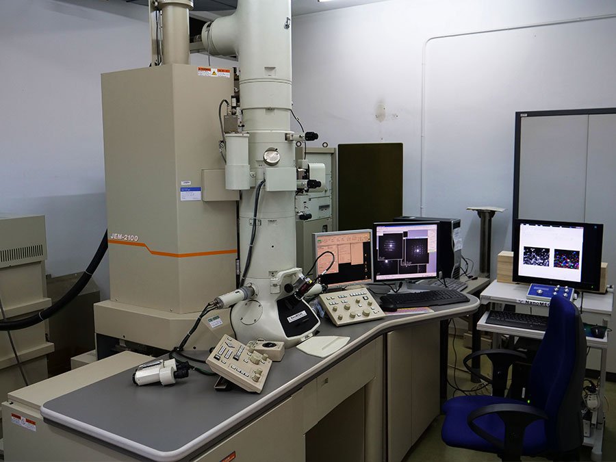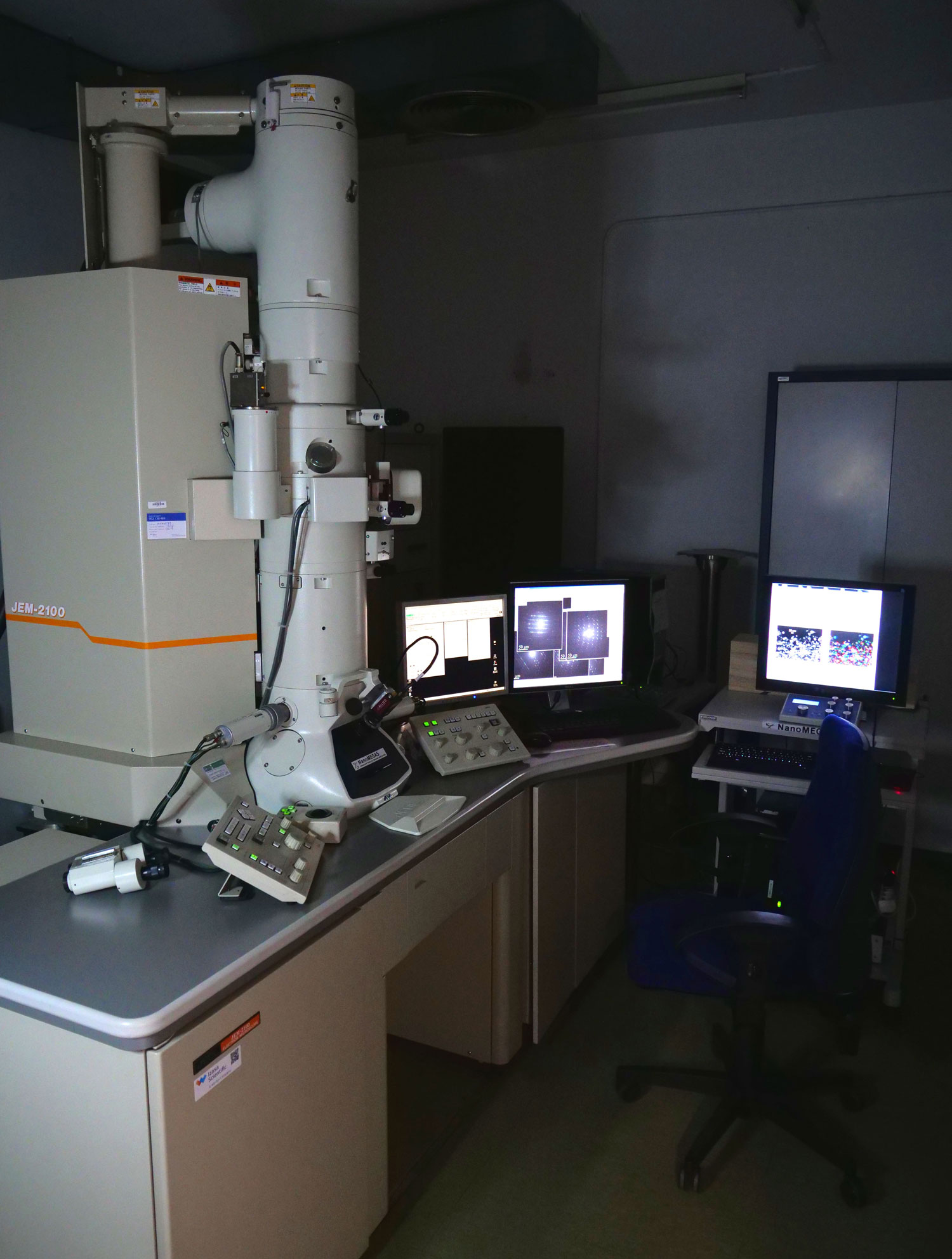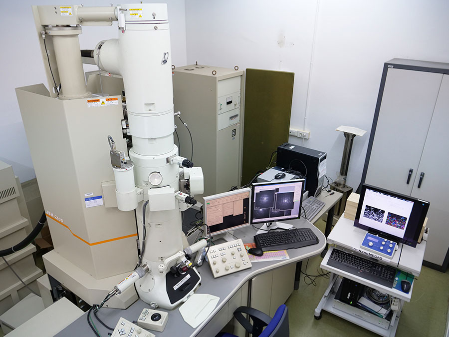
Jem 2100
The JEM2100 microscope is a versatile tool that allows characterizing a wide range of samples both from Materials Science and Life Sciences. Morphological and structural information can be obtained in imaging mode (HRTEM) as well as from diffraction (SAED or PED) and chemical composition can be mapped using XEDS spectroscopy.
USES OF THE EQUIPMENT
- Morphological characterization of samples both from Materials Science and Life Sciences
- Structural characterization of crystalline materials (HRTEM, SAED, PED)
- Chemical mapping (STEM-EDX)
- Crystal orientation and phase mapping (ASTAR)
- Strain mapping (TOPSPIN)
TECHNICAL SPECIFICATIONS
- Accelerating voltage: 120 kV – 200 kV
- Thermionic emission LaB6 filament
- CCD camera: Gatan ORIUS SC1000A
- STEM unit with bright field (BF) and high angle annular dark field (HAADF) detectors
- XEDS microanalysis system (Oxford Instruments)
- Electron beam precession system (DIGISTAR)
- Phase and crystal orientation mapping system (ASTAR)
- Crystal strain mapping system (TOPSPIN)
- JEOL tomography holder (±70o)
- Nanofactory TEM-STM holder for in situ electrical measurements