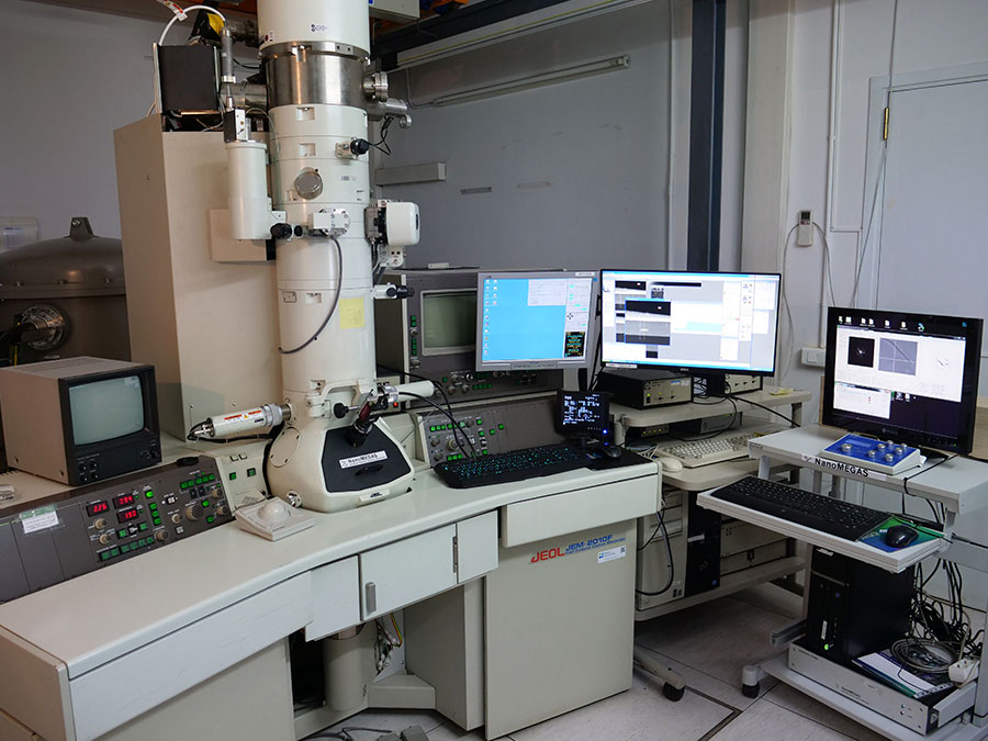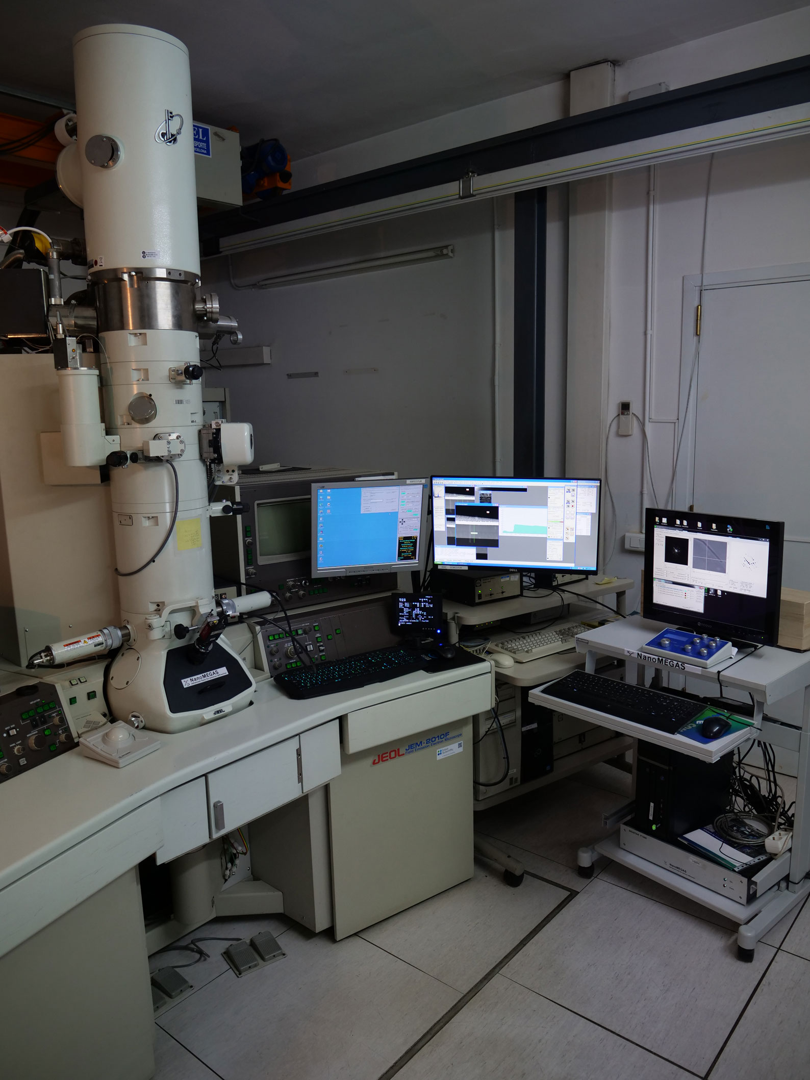
JEM 2010F
The JEM2010F microscope is equipped with a field emission electron gun, giving a higher intensity and better resolution in parallel beam mode (HRTEM) and in scanning mode (STEM).
The microscope has an energy filter for the analysis of the electron energy loss. Electron energy loss spectroscopy (EELS) not only allows mapping the chemical composition of the sample under study, but also studying valence and coordination states through the analysis of the near-edge fine structure, or accessing optoelectronic properties of materials through the study of the low loss energy range of the spectra.
USES OF THE EQUIPMENT
- Obtaining HRTEM images from crystalline materials (nanoparticles, nanowires, thin films, etc.)
- Chemical mapping (STEM-EELS)
- Mapeado de fases y orientaciones cristalinas (ASTAR)
- Mapeado de tensiones cristalinas (TOPSPIN)
TECHNICAL SPECIFICATIONS
- Accelerating voltage: 200 kV
- Field emission electron gun (FEG)
- CCD camera: Gatan ORIUS SC200
- STEM unit with bright field (BF) and high angle annular dark field (HAADF) detectors
- Energy filter for the study of electron energy loss (GIF)
- Electron beam precession system (DIGISTAR)
- Phase and crystal orientation mapping system (ASTAR)
- Crystal strain mapping system (TOPSPIN)
- JEOL tomography holder (±70o)
- Nanofactory TEM-STM holder for in situ electrical measurements